

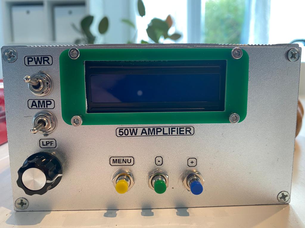
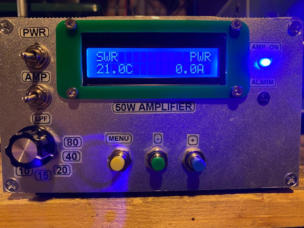
Amplifier Controller
For my tiny 30w MOSFET and LDMOS amplifier equipped with LPF, i need few features in order to operate smoothly and securely this device.
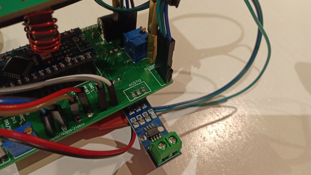
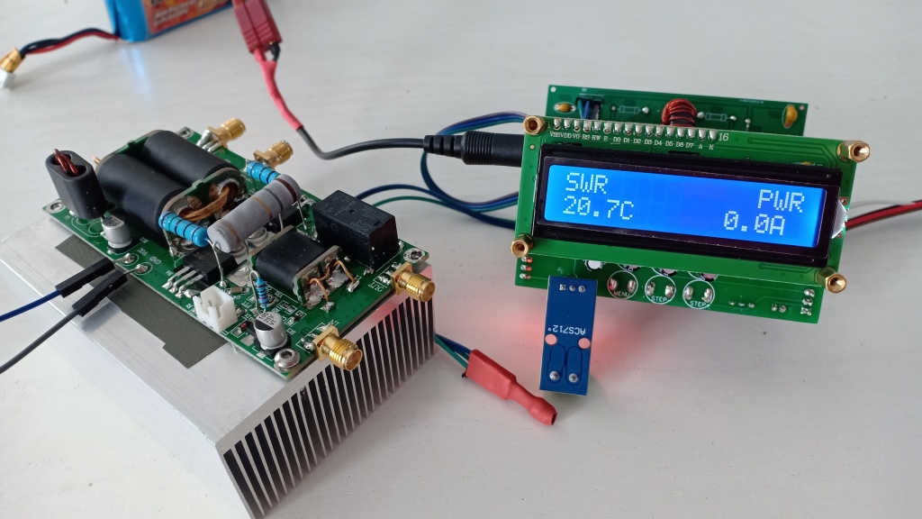
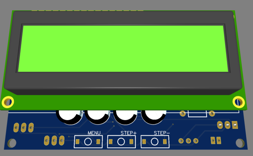
-Amplifier control : Temperature , SWR , Bias , Current & Voltage control with alarm and security trigger using an ARDUINO NANO.
The full package : Gerber , BOM, kicad , pictures, and arduino Sketch for the main controller and the SWR bridge : https://drive.google.com/file/d/1OAA3AwHDP3Jk_RUIIhog9YnVMdybFQ75/view?usp=sharing

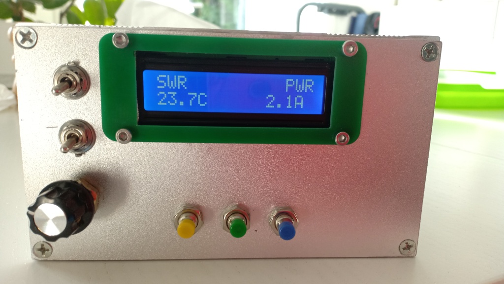
The controller is monitoring the amplifier current and obviously the SWR and output power
- The amplifier is biased with 3.7vdc with about 70ma quiescent current –> input power is 1w for about 40 up to 55w output
- The controller is providing the following capabilites:
- Temperature monitoring with dedicated menu to adjust the threshold to trigger a 12vdc Fan
- Current monitoring with a dedicated menu to adjust the max amp (Limitation) in order to cut-off the biasing with an opto relay when the current is too high
- A dedicated menu for the Max SWR adjusment –> It will trigger the opto relay to cut-off the biasing
- A dedicated menu to adjust the output power range you want to monitor . Since the power is about 50w , my adjusment is 100w which is tailoring the bargraph display accordingly.
- Using FT50-43 toroids and 5w 50ohm resistor, the SWR bridge able to handle up to 1Kw
Currently i am using MOSFET amplifier for 3 years with this kind of controller with another amplifier and working perfectly.
https://easyeda.com/F5NPV/swr-meter

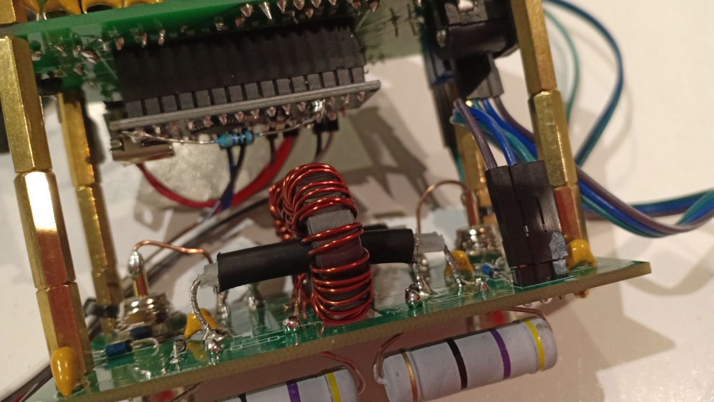
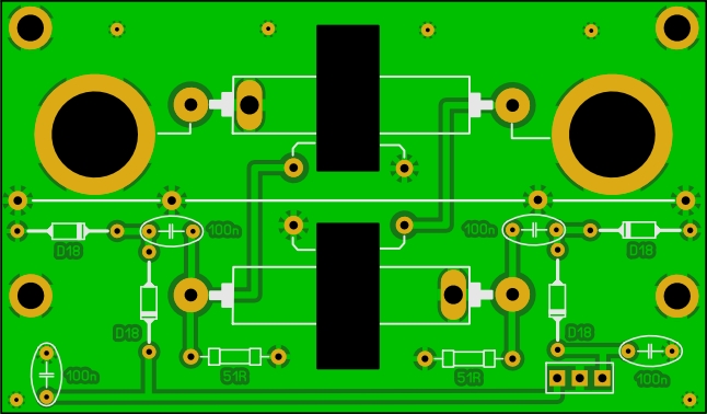
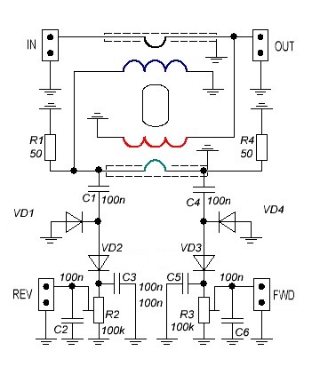
For VD Diodes , i am using BAT41 diodes or 1N5711 . For R1 and R4 since i do not have 50R Resistor , i am using 47R 5w resistor . The Menu is offering to adjust the Resistor Value.
The gerber file for the SWR bridge : https://drive.google.com/file/d/1i1FAbeb4EyGl6EbUAo1TmMHviFV_yVLi/view?usp=sharing
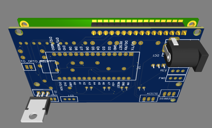
Since i have this kind of relay , this is an easy integration for the opto relay output.

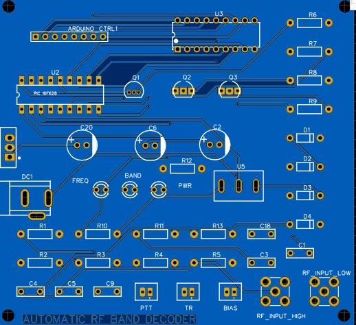
Automatic band decoding with RF Detection
This is the VK5TM’s design populated for easy implementation.
More details and gerber files are here : https://easyeda.com/F5NPV
The main purpose of this circuit is to provide automatic band switching capabilities for LPF to any radio rig. The main principle is RF detection during tuning and use the PIC as a frequency counter and switch. All my tests and experimentation was performed with TINYSA , a NANOVNA or a SARK100 on the high level RF input.
The final implementation i am using the Low level input with a ferrite core . i wrap few turn on the core to achieve a RF sample to the PIC (You need to test according the core you are using)
I have included the following features:
-PTT circuit
-High level RF input (You can tap directly on your low power input from 1 to 5w)
-Low level RF input (a simple tiny antenna is sufficient or few turns on a ferrite core)
-A switch in order to switch the RF level input . I am using a 2P switch with a middle neutral position to cancel any RF input.
-Instead of using an ULN2803 , i am using an ULN2804 since my LPF are all using 12vdc relays
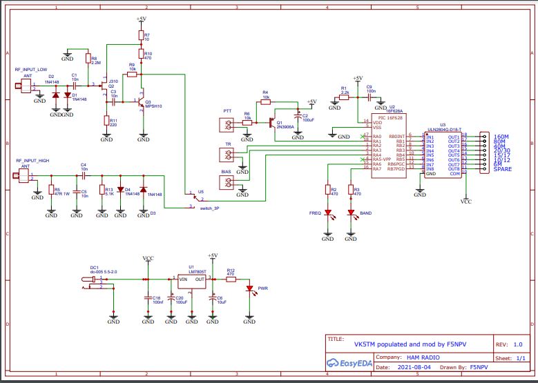
https://www.vk5tm.com/homebrew/freq_switch/freq_switch.php
I am using this design with my 30w Mosfet and 300w LDMOS amplifiers. So far this system is working quit well

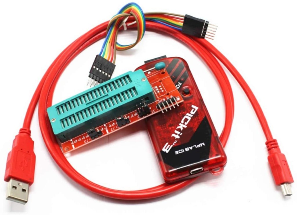
My Pickit3 Tool :
All will be populated all in one , so stay tuned for the final result ………….
The PIC16F628A I/F ASM code
;********************************************************************
; 		VK5TM Frequency Dependant Switch
;			VK5TM_FDS_PTTV0_3.asm
;
; Original code & hardware design by Peter Rhodes, BSc, G3XJP
; See RSGB Radcom magazine Sep to Dec 2001
;
; Modified by Terry Mowles VK5TM Aug 2019
;
; Modifications:
;	Remove EEProm storage of variables - converted to tables.
;	Remove changing variables using jumper method.
;	Works from PTT activation only.
;	Converted to 16F628A running on internal oscillator.
;	Changed filter outputs to all PortB.
;	Rearranged all other inputs/outputs to PortA.
;********************************************************************
	errorlevel -302, -305  ; Skip nuisance messages

	LIST 		P=PIC16F628A

	INCLUDE		P16F628A.inc

	__config _CP_OFF&_LVP_OFF&_BODEN_OFF&_MCLRE_OFF&_PWRTE_ON&_WDT_OFF&_INTOSC_OSC_NOCLKOUT

#define	PTT		PORTA,1
#define	TR_relay	PORTA,2
#define	bias		PORTA,3
#define	RF		PORTA,4
#define	LED1		PORTA,6	; Frequency measured
#define	LED2		PORTA,7	; Channel change


;	decimal #'s following equal time in mS (approx)
#define tA		d'15'		; T/R relay operate delay time
#define tB		d'15'		; bandsw relay operate time
#define tC		d'8'		; bandsw relay release time
#define tD		d'20'		; Bias operate delay
#define tE		d'10'		; Debounce time

	CBLOCK	0x20	; Start Data Block

	delay1		; misc counters for use in time delays
	delay2
	delay3
	freq		; cache for freq count
	repeat		; number of extra times freq is counted
	oldCh		; last channel in use
	temp		; general purpose transient variable
	r_data

	endc
;;;;;;;;;;;;;;;;;;;;;;;;;;;;;;;;;;;;;;;;;;;;;;;;;;;;;;;;;;;;;;;;;;;;;;;;;;;;;;;;;;;;;;;;
	org	0
	goto	main
	org	4
	goto	main

channel;
	addwf	PCL,f		; Band Count	Dest
	retlw	b'00100000'	; 10m -> initial start-up band
	retlw	b'00000001'	; 160m	1	RB0
	retlw	b'00000010'	; 80m	2	RB1
	retlw	0		;	3	error
	retlw	b'00000100'	; 40m	4	RB2
	retlw	b'00001000'	; 30m	5	RB3
	retlw	b'00001000'	; 30m	6	RB3
	retlw	0		;	7	error
	retlw	b'00001000' 	; 20m	8	RB3
	retlw	0		;	9	error
	retlw	b'00010000'	; 17m	10	RB4
	retlw	0		;	11	error
	retlw	b'00010000'	; 15m	12	RB4
	retlw	0		;	13	error
	retlw	b'00100000'	; 12m	14	RB5
	retlw	0		;	15	error
	retlw	b'00100000'	; 10m	16	RB5
	retlw	b'00100000'	; 10m	17	RB5

main
	clrf	PORTA		; initialise
	clrf	PORTB		; initialise
	movlw	0x07		;
	movwf	CMCON		; Turn off comparators
	bsf	STATUS,RP0	; to Bank 1
	movlw	b'10100111'	; prescale /256 to RA4, no pull-ups
	movwf	OPTION_REG
	movlw	b'00010010'	; RA1 & RA4=input
	movwf	TRISA
	clrf	TRISB		; PortB all outputs
	bcf	STATUS,RP0	; back to Bank 0

	movlw	0		; initialise startup band
	call	channel
	movwf	r_data
	call	new_Ch		; do it!

initialise 			; clear all outputs (except filter) to Rx state

	bcf	bias		; turn off bias output
	movlw	tC		; Relay release time
	call	w_mS		;
	bcf	TR_relay	; turn off T/R relay after delay
	nop			; nop for port read/modify/write problem
	bcf	LED2
	nop
	bcf	LED1

wait_Tx
	btfsc	PTT		; is PTT activated?
	goto	wait_Tx		; if not, go back and wait

	movlw	tE		; PTT debounce
	call	w_mS
	btfsc	PTT
	goto 	wait_Tx

	btfsc	RF		; Wait for RF input
	goto	$-1

;  Measure freq.  Potential errors are:-
; 	Tx stops/starts while measuring
; 	out of band measure
; 	no count, not enough power
; 	successive counts not same
	movlw	d'4'
	movwf	repeat		; # times to repeat
	call	freqcount	; measure once
	movwf	freq		; and retain
	btfsc	STATUS,Z	; test for zero
	goto	initialise	; zero or > 10m error
	bsf	LED1		; light Frequency measured LED
freq_again
	call	freqcount	; measure again
	subwf	freq,w		; compare
	btfss	STATUS,Z	; same?
	goto	initialise	; not same freq error
	decfsz	repeat		; all done?
	goto	freq_again	; no, so loop
	movf	freq,w		; yes, all OK, continue

	call	channel
	movwf	r_data
	iorlw	0x00		; Test if 'W' is 0
	btfsc	STATUS,Z	; zero?
	goto	initialise	; yes out of band error

	subwf	oldCh,w		; compare old
	btfss	STATUS,Z	; same?
	call	new_Ch		; it is different

	movlw	tA		; T/R relay time
	call	w_mS		; and delay for w mS
	bsf	TR_relay	; to transmit

	movlw	tD		; Bias relay delay time
	call	w_mS		; and delay for w mS
	bsf	bias		; turn bias on
	nop
	bcf	LED2		; and LED2 Channel change off

	btfss	PTT		; wait for PTT to be released
	goto	$-1

	goto	initialise

; FREQUENCY COUNT
freqcount
	clrf	TMR0		; reset & start count
	call	delay_150uS
	movf	TMR0,w		; end & latch result
	movwf	temp		; preserve w
	sublw	d'17'		; max legal count
	btfss	STATUS,C	; test for >max?
	clrf	temp		; count was >max
	movf	temp,w		; recover w
	return			; with count in w (0 if error)

new_Ch	; NEW CHANNEL NEEDED
	bsf	LED2		; Channel change LED on
	movf	r_data,w	; get new Ch
	movwf	oldCh		; overwrite old
	iorwf	PORTB,f		; start 'make' new
	movlw	tB 		; operate time
	call	w_mS		; complete 'make'
				; break old channel
	movf	oldCh,w		; now current Ch
	movwf	PORTB
	return

delay_150uS
;PIC Time Delay = 0.00014900 s with Osc = 4,000,000 Hz
	movlw	D'48'		; Adjust up or down if BIAS LED
	movwf	delay1		; doesn't light on some channels
				; or band switching is intermittent on some bands
loop
	decfsz	delay1,f
	goto	loop
	return
;
; DELAY LOOP 1 millisecond
one_mS
	movlw	d'4'
	movwf	delay1
loop1
	movlw	d'81'
	movwf	delay2
loop2
	decfsz	delay2
	goto	loop2
	decfsz	delay1
	goto	loop1
	return

; DELAY LOOP w milliseconds (roughly)
w_mS
	movwf	delay3
w_mS_loop
	call	one_mS
	decfsz	delay3
	goto	w_mS_loop
	return

	END
;--------------------------------------------------------------------------------

hello didier
I noticed that in the Automatic Band decoder, the pin connection of your MPSH10 seems to be different from that of the original author’s VK5TM? In your circuit the RA4 pin of the PIC is grounded. Can both circuits be used normally?
73
Trendy
LikeLike
Hello Trendy,
i have corrected the schematic months ago but forgot to update the website but on EASYEDA the schematic is correct. i put mow the correct schematic on the website.
73s Didier
LikeLike
Thank you, didier.
I noticed that your PTT interface should be active at low level. When the PTT terminal is shorted, the control circuit takes effect, right?
And I also noticed that it seems that the schematic on easyEDA is still wrong, it seems that you forgot to correct it.
73
Trendy
LikeLike
Hello,
Yes the PTT is active when pulled low (Shorted with the ground) and will trigger the frequency counting from the PIC.
Currently i have a very limited spare time due to my office work. can you please pinpoint where there is an error. Reccently VK5TM had reviewed the schematic and the only error he had noticed was regarding MPSH10.
i will be able to work on this coming week end , during weekday i am terribly busy for now .
My email adress if you can send me more details , a modified shematic (the schematic from EASYEDA can be downloaded and modified)
73s
LikeLike
Hello Again,
Ok i manage to find the issue and was regarding the output from the MPSH10 to RA4 . i have modified the easyda Sheet and PCB
73S
Didier
LikeLike
Thank you again, didier
Thank you very much for taking time out of your busy schedule to reply to me.
I noticed that the schematic diagram on your webpage has modified the RA4 pin to be the same as VK5TM, so I will take the schematic diagram on this website as the standard. RA4 should be connected to collector of MPSH10, right?
But it seems that you forgot to save the modification on easyEDA. When I enter easy EDA to check, it still has not changed.
In addition, the RF_INPUT_LOW you mentioned refers to winding the enameled wire on the magnetic ring for a certain number of turns, then passing through the RF input wire, and connecting the two ends of the enameled wire to the “RF_INPUT_LOW” port, is it?
Good luck with your work.
73
Trendy
LikeLike
Hello,
i think there is an issue with EASYEDA website because when you open the schematic with the editor you will find the corrected one. Yesterday when i modified the schematic with the editor it takes for ever to save it.
i will try again after after work to figure out why the schematic on the main EASYEDA web page is not taking into account the modify schematic from the EASYEDA editor.
73s Didier
LikeLike
Hello Didier
I checked EasyEDA again and found that it has been updated.
Regarding the “RF_INPUT_LOW” port problem I mentioned, is it correct? Looking forward to your reply.
Thank you again.
73
Trendy
LikeLike
Hello,
Yes this the RF_INPUT_LOW and the output of the MPSH10 transistor
73s Didier
LikeLike
Hello Didier
For RF_INPUT_LOW, how many turns on the ring do you think I should try initially? I may use FT50-43 magnetic ring.
Also if you are free, I hope you can upload a video of the power amplifier with automatic band selection on youtube. It’s okay if you’re busy all the time.
Thank you once again.
73
Trendy
LikeLike
Hello,
you will need to make some test. Myself i use generally 20 to 30 turns. They main concern it to avoid voltage above 5v peak to peak if the output of the ring average is about 2 volts peak to peak is fine.
73s Didier
LikeLike
OK,I see.
Thank you.
73
Trendy
LikeLike
Hi, on Amp Controller schematic variable resistor values shown as 50K but the part number is 10Ohm. Which one is correct value?
LikeLike
Hello ,
it is 50k variable resistor
73s Didier
LikeLike
I have checked again, the sketch you have given, does not detect the DS18B20 nor the ACS712 in the circuit you have published. also all the switches are operating as menu. can you please send me a checked and updated firmware, it will be a great help. my email id is deynet@gmail.com. my call VU3FBT
LikeLike